Wednesday, January 1, 2020

Getting Started with High-Speed PCB Design, Beginners Must Understand These 10 Concepts

Getting Started with High-Speed PCB Design, Beginners Must Understand These 10 Concepts

PCBA
To learn high-speed PCB design, firstly you must understand some basic concepts, such as what is electromagnetic interference (EMI)? What is Signal Integrity (SI)? What is reflection? Laying the foundation for faster entry into the high-speed PCB design.

 Electromagnetic interference (EMI)

Electromagnetic Interference (EMI) is an electronic noise that interferes with cable signals and reduces signal integrity. EMI is typically generated by sources of electromagnetic radiation such as motors and machines.

Electromagnetic Interference EMI has both conducted and radiated interference. Conducted interference refers to the coupling (interference) of signals on one electrical network to another electrical network through a conductive medium. Radiated interference refers to an interference source that couples (interferes) its signal to another electrical network through space. In high-speed PCB and system design, high-frequency signal lines, integrated circuit pins, various types of connectors, etc. may become radiation interference sources with antenna characteristics, which can emit electromagnetic waves and affect other systems or other subsystems in the system. normal work.

Electromagnetic compatibility (EMC)

Electromagnetic compatibility (EMC) refers to the ability of a device or system to operate in its electromagnetic environment without causing unacceptable electromagnetic disturbances to any device in its environment. Therefore, EMC includes two requirements: on the one hand, the electromagnetic disturbance of the equipment in the normal operation process (Electromagnetic Disturbance) can not exceed a certain limit; on the other hand, the equipment exists in the environment Electromagnetic disturbance has a certain degree of immunity, namely Electromagnetic Susceptibility (EMS).

The International Electrotechnical Commission (IEC) defines EMC as: Signals and interference can coexist without damaging the information contained in the signal.

 Signal integrity refers to the quality of a signal on a signal line. Signals with good signal integrity are those that have to be reached when needed. Poor signal integrity is not caused by a single factor, but by a combination of factors in the board design. The main signal integrity issues include reflection, oscillation, ground bounce, crosstalk, and so on.

Power Integrity (PI)

Power integrity, referred to as PI, is to confirm whether the voltage and current of the source and destination of the power supply meet the requirements. Power integrity is important in today's electronics. There are several levels of power integrity: chip level, chip package level, board level, and system level. The power integrity at the board level meets the following three requirements:

  1. Make the voltage ripple of the chip pin smaller than the specification (for example, the error between voltage and 1V is less than +/-50 mV)

  1. Control ground bounce (also known as synchronous switching noise SSN, synchronous switching output SSO)

  1. Reduce electromagnetic interference (EMI) and maintain electromagnetic compatibility (EMC): The Power Distribution Network (PDN) is the largest conductor on the board and therefore the antenna that is the easiest to transmit and receive noise.

PCBA

Crosstalk

Crosstalk is the coupling between two signal lines. The mutual inductance and mutual capacitance between the signal lines cause noise on the line. Capacitive coupling induces a coupling current, while inductive coupling induces a coupling voltage. PCB board layer parameters, signal line spacing, electrical characteristics of the driver and receiver terminals, and line termination methods all have a certain impact on crosstalk.

Reflection

Reflection is the echo on the transmission line. A portion of the signal power (voltage and current) is transmitted to the line and reaches the load, but a portion is reflected. If the source and load have the same impedance, the reflection will not occur. A mismatch between the source and load impedance causes on-line reflections, and the load reflects a portion of the voltage back to the source. If the load impedance is less than the source impedance, the reflected voltage is negative. Conversely, if the load impedance is greater than the source impedance, the reflected voltage is positive. Such reflections can be caused by variations in wiring geometry, incorrect wire termination, transmission through the connector, and discontinuity in the power plane.

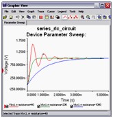
Overshoot and undershoot

Overshoot is the first peak or valley value that exceeds the set voltage—for the rising edge, the highest voltage and for the falling edge, the lowest voltage. Undershoot is the next valley or peak. Excessive overshoot can cause the protection diode to work, leading to premature failure. Excessive undershoot can cause false clock or data errors (mis-operating).

Ringing and rounding

The phenomenon of oscillation is repeated overshoot and undershoot. The oscillation of the signal and the surrounding oscillation are caused by excessive inductance and capacitance on the line. The oscillation belongs to the underdamped state and the surrounding oscillation belongs to the overdamped state. Signal integrity problems typically occur in periodic signals, such as clocks. Oscillation and surround oscillations are caused by a variety of factors, as are reflections. Oscillation can be reduced by proper termination, but it cannot be completely eliminated.

Courtesy
Rayming PCB

Friday, September 20, 2019

Enhancement Mode MOSFET & Depletion Mode MOSFET

The Main difference between these MOSFET is given below,

Enhancement Mode MOSFET is generally an open Switch, In 0 V the MOSFET is in OFF condition.  To switch ON the Transistor we need to apply VGS.

Depletion Mode MOSFET is generally a Closed Switch, In 0V its conducting, and its in ON condition.

To Switch OFF the transistor we need to apply VGS.

Friday, June 21, 2019

Hydrogen Powered train

https://www.dailymail.co.uk/sciencetech/article-7161839/Britains-hydrogen-powered-locomotive.html

Tuesday, June 18, 2019

SPICE Analysis

TRANSIENT ANALYSIS

Transient analysis is the analysis of the circuits during the time it changes from one steady state condition to another steady state condition. Transient analysis will reveal how the currents and voltages are changing during the transient period.


DC ANALYSIS

DC Operating Point Analysis calculates the behavior of a circuit when a DC voltage or current is applied to it. The result of this analysis is generally referred as the bias point or quiescent point, Q-point. In most cases, the results of the DC Operating PointAnalysis are intermediate values for further analysis

Table of Contents

  1. DC Operating Point Analysis
  2. DC Sweep Analysis
  3. Transient Analysis
  4. AC Analysis
  5. Temperature Sweep Analysis
  6. Fourier Analysis
  7. Worst Case Analysis
  8. Noise Analysis
  9. Noise Figure Analysis
  10. Parameter Sweep Analysis
  11. Additional Resources

DC Operating Point Analysis

DC Operating Point Analysis calculates the behavior of a circuit when a DC voltage or current is applied to it. The result of this analysis is generally referred as the bias point or quiescent point, Q-point. In most cases, the results of the DC Operating Point Analysis are intermediate values for further analysis.
Back to top

DC Sweep Analysis

DC Sweep Analysis is used to calculate a circuits’ bias point over a range of values. This procedure allows you to simulate a circuit many times, sweeping the DC values within a predetermined range. You can control the source values by choosing the start and stop values and the increment for the DC range. The bias point of the circuit is calculated for each value of the sweep.  

Back to top

Transient Analysis

In Transient Analysis Multisim computes the circuit’s response as a function of time. This analysis divides the time into segments and calculates the voltage and current levels for each given interval. Finally, the results, voltage versus time, are presented in the Grapher View.
Back to top

AC Analysis

AC Analysis is used  to calculate the small-signal response of a circuit. In AC Analysis, the DC operating point is first calculated to obtain linear, small-signal models for all nonlinear components. Then, the equivalent circuit is analyzed from a start to a stop frequency. The result of an AC Analysis is displayed in two parts: gain versus frequency and phase versus frequency.

Back to top

Temperature Sweep Analysis

Using Temperature Sweep Analysis you can quickly verify the operation of your circuit by simulating it at different temperatures. The effect is the same as simulating the circuit several times, once for each temperature. You control the temperature values by choosing start, stop and increment values.

Back to top

Fourier Analysis

Fourier Analysis is a method of analyzing complex periodic waveforms. It permits any nonsinusoidal period  function to be resolved into sine or cosine waves, possibly an infinite number, and a DC component. This permits further analysis and allows you to determine the effect of combining the waveform with other signals.

Back to top

Worst Case Analysis

Worst Case Analysis is a statistical technique that uses a “what if” approach to provide a practical result and its primary purpose is to identify the most critical components of a circuit. This analysis helps you answer the question: What will be the worst possible effects of variations in component parameters?     

Back to top

Noise Analysis

Noise Analysis calculates the noise contribution from each resistor and semiconductor device at the specified output node. Multisim creates a noise model of the circuit using noise models of each resistor and semiconductor devices and then performs AC-like analysis. It calculates the noise contribution of each component and propagates it to the output of the circuit sweeping through the frequency range specified. 

Back to top

Noise Figure Analysis

Noise Figure Analysis is used to specify exactly how noisy a device is. For a transistor, noise figure is simply a measure of how much noise the transistor adds to the signal during the amplification process. In a circuit network, the noise figure is used as a figure of merit to compare the noise in a network with the noise in an ideal or noiseless network. It is a measure of the degradation in signal-to-noise ratio (SNR) between the input and output ports of a network.

Back to top

Parameter Sweep Analysis

With Parameter Sweep Analysis you can verify the operation of a circuit by simulation across a range of values for a component parameter. The effect is the same as simulating the circuit several times, once for each value. You control the parameter values by choosing a start value, end value, type of sweep that you wish to simulate and the desired increment value.

Thursday, June 13, 2019

A-faster-way-to-rearrange-atoms

https://spectrum.ieee.org/nanoclast/semiconductors/nanotechnology/a-faster-way-to-rearrange-atoms

Getting Started with High-Speed PCB Design, Beginners Must Understand These 10 Concepts

Getting  S tarted with  H igh- S peed PCB  D esign,  B eginners  M ust  U nderstand  T hese 10  C oncepts To learn  high-speed PCB de...